Behind the scenes at RoodMicrotec!
| This mail contains images. Alternatively you can watch the web version | ||
 |
||
| www.roodmicrotec.com | May 2026 | ||
| Dear Reader, I am happy to introduce this year's second edition of RoodMicrotec's newsletter. In this issue, we will let you have a look behind the scenes at RoodMicrotec and give you an insight into our enhanced wafer testing flow and also inform you about new developments.
Wishing you lots of reading enjoyment. Yours sincerely, Jan de Koning Gans Managing Director - Sales & Marketing |
||
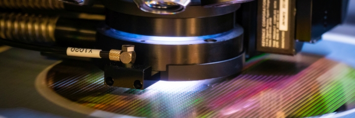
Professional test and precise analysis supportPCM Analysis
During the wafer manufacturing process, parameters are monitored with PCM (Process Control Monitor) structures. PCM is data that is collected at the end of the actual wafer fabrication process. Before wafer shipment, the foundry provides PCM data for further detail analysis. Thereby, trends (process shift) and mavericks can be detected. It is very important to analyze pass or fail, contact resistance, sheet resistance, Zener Breakdown, voltages and other parameters. Any process shift can be detected and the foundry will be informed immediately to correct the process of further lot manufacturing and, if necessary, to stop the shipment of an affected lot for analysis of usability. If the lot is not acceptable, RoodMicrotec can stop the subsequent wafer test. This method saves time and money for both parties - RoodMicrotec and the customer. Below you can see examples of a few PCM parameters: Pass or fail, contact and sheet resistance criteria for NMOS and PMOS:
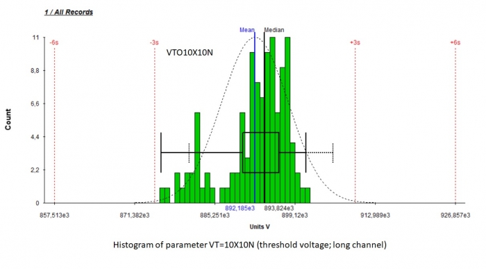 (Source: RoodMicrotec) All values are clearly within 3 sigma range. Wafer Test If the PCM data analysis is finished and all parameters passed the limits,the wafer test is executed according to the test specification. Each implemented module - analog, digital or RF - is clearly defined within the customer's wafer test specification. From the wafer test, we get all defined and measured electrical parameters' readings. Based on the test results, we produce a wafer map. With this wafer map, the pass components are picked up for assembly.
Final Device Test Final test will be runned according to the final test specification. The data analysis method is similar to that at wafer test. Analysis and Yield Monitoring The complete data analysis for PCM, wafer and final test is carried out with DataView from Test Spectrum. Our standard visualization procedure includes Histogram, TrendView, Scatter View and BIN View. If we see problems with any parameter, we can react and advise precisely. Customers will benefit from our professional data analysis and continuous yield monitoring during ramp up phase and production. 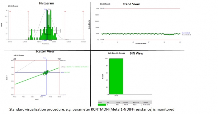 (Source: RoodMicrotec) |
||
AOI System for 6, 8 and 12 inch wafersIn the first quarter of 2019, a new automatic optical inspection (AOI) system for semiconductor wafers has been installed in our test facility in Nördlingen. The STI iFocus 505, a state-of-the-art system, adds a wide range of new possibilities to the company's portfolio of services.
With this new capability, we will have a solution that fits the requirements of our customers, especially in the automotive sector. The purpose of this service is to detect failures and damages on incoming wafers as well as the quality assurance of outgoing wafers. It will enable us to identify possible defects resulting from earlier processing steps, such as wafer manufacturing or transport, and to deliver products of the best possible quality. The AOI system is able to automatically handle 6, 8 and 12 inch wafers from cassette to cassette. It also offers the possibility to handle and inspect whole or partial wafers mounted on film frame. The two main parts of the system are the handling-unit and the vision-unit. The handling-unit consists of a robot that handles the wafers and guides them from the cassette to the vision-unit. The vision-unit includes the movable chuck on high precision linear motors and the powerful vision system right on top of it. The complete system is mounted on a block of granite weighing half a ton and lying on four air dampers to provide the necessary stability and to compensate for vibrations. The throughput of the system depends on the magnification applied. Mainly, 5X is used, but the machine is also capable of 2.5X, 3.5X, 7.5X, and 10X.
The magnification determines the size of defects that can be detected. At 10X for example, defects of a size of 1.6µm x 1.6µm can be found. 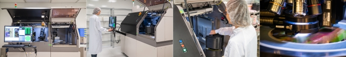 (Source: RoodMicrotec)
|
||
RoodMicrotec at the NordPac ConferenceRoodMicrotec attended the NordPac Conference on Microelectronics Packaging at DTU - Technical University of Denmark on June 11-13. Our colleagues Jan de Koning Gans and Jürgen Gruber were on site with a booth presenting our services. Additionally, Jürgen Gruber was one of the speakers at the conference with 'From the Failure Analysis to Anamnesis and its Feedback to Qualification Procedures'. His presentation and discussion were well received by the audience.
The conference was a good opportunity to meet new people and present RoodMicrotec's portfolio. 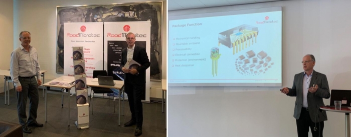 (Source: RoodMicrotec)
|
||
New faces - We got personnel reinforcement!We are proud to announce that our team has just grown larger as we welcome two new team members - Christian and Oliver - who will strengthen our team with extensive competence in the field of failure analysis and internal sales.
To get to know them better, we asked them the following three questions: 1. What are you doing at RoodMicrotec? 2. How does your daily work life look like? 3. What is your RoodMicrotec highlight so far? Christian 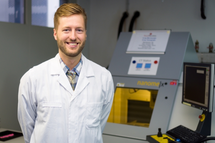 1. My basic work consists of performing module and failure analysis of highly sensitive electrical components. For the analysis, it is necessary to devise a concrete plan to achieve the desired result by means of, for example, wet-chemical methods or basic craft activities, such as grinding and soldering.
2. There are certain rules to follow during your activities, if a company is certified and accredited. However, these rules give me some leeway in what I do and how to solve a problem. Besides, I have colleagues with outstanding expertise, who help me tremendously with my day-to-day work and to develop professional and personal skills. 3. I haven't experienced an outstanding highlight so far, but the repetitive pizza lunch and the Friday burgers with my colleagues provide a welcome change from the working day. However, it's been a great pleasure for me to satisfy my first customers because of my lab work, with my reports or during phone calls. Moreover, finding the root cause for failure is a small personal highlight, but certainly, this is exactly our customers' demand. Oliver 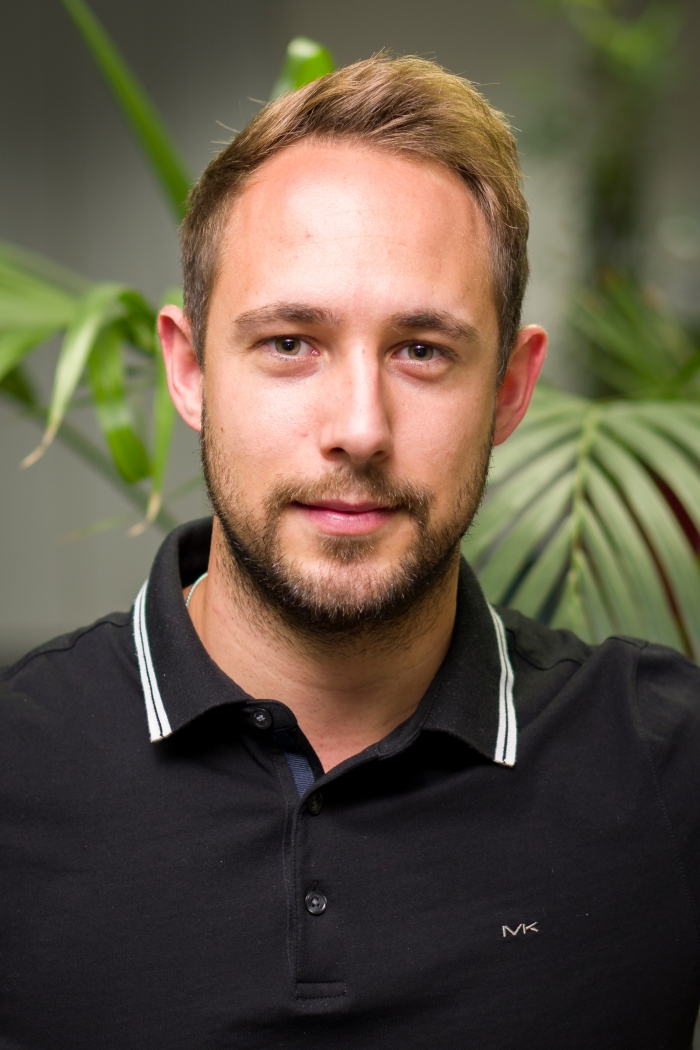 1. I work in the internal sales team.
2. I receive customer inquiries, analyze the requirements, discuss them with the relevant departments, and check the requests for their technical feasability. Then, I calculate them. If everything is calculated, I send our offer to the customer. 3. My biggest highlight was to participate in a meeting about a big project just a few days after my start in the company. |
||
Update of forthcoming eventsOctober 1 AESIN Conference (Birmingham, UK) October 10 RoodMicrotec Seminar on Electrical Overstress (EOS) (Stuttgart, GER) |
||
RoodMicrotec GmbH | Oettinger Str. 6 | 86720 Nördlingen/ Germany Tel.: +49 (0) 9081 804-0 | [email protected] |
||
| If you no longer wish to receive our newsletter, please unsubscribe here | ||