News from RoodMicrotec
| This mail contains images. Alternatively you can watch the web version | ||
 |
||
| www.roodmicrotec.com | | ||
| Dear Reader,
Have you ever heard of the term press-fit connection? It is a special connection technique for solderless contacting between printed circuit boards and mechanical connecting elements such as plugs or power terminals. We at RoodMicrotec offer press-fit pin & PCB qualifications in compliance with common approval guidelines of OEMs or Tier1 suppliers. In our second issue, you will learn more about this special connection technique. I wish you an interesting reading. All the best from Jan de Koning Gans Managing Director - Sales & Marketing |
||
Qualification of press-fit connectors and PCBsPress-fit connections have become a reliable connection technology with good electrical and mechanical properties, especially in the automotive industry. They offer a robust, solder-free connection between PCBs and connectors or a connection on module level.To establish the connection, flexible pins are pressed into vias of the PCB. Many factors contribute to a reliable press-fit connection. The geometries of the pin and the via need to be aligned.The press-in process must be well characterized in terms of press-in force and final pin position.The metallization of the via and the PCB layers itself need to withstand the deformation during the process. Whisker growth has to be quantified. Depending on customer-specific requirements, many more tests are needed before releasing a press-fit pin or PCB for production.
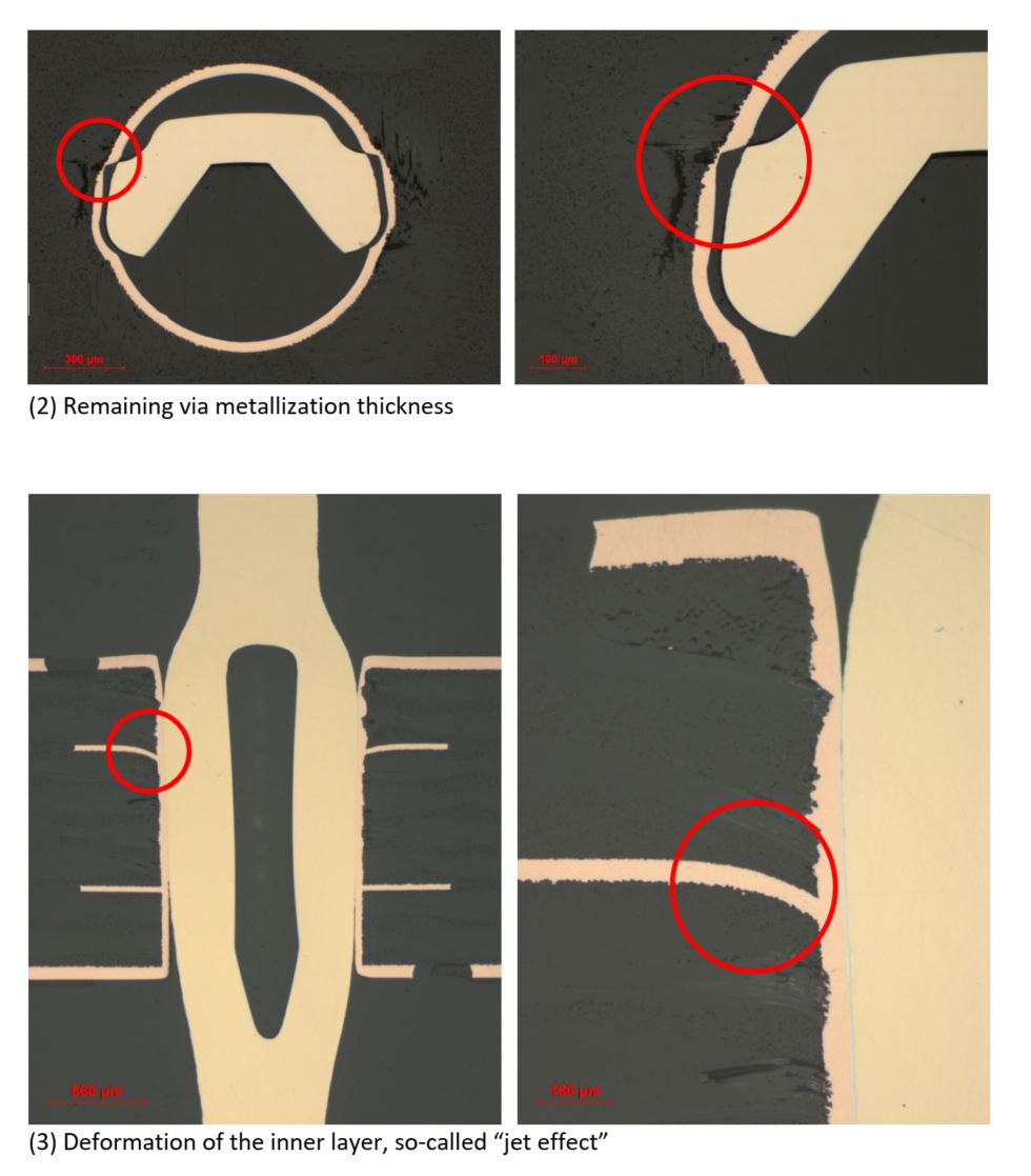
With our extensive knowledge and equipment, we are able to perform the complete test plans of large OEMs or Tier1 suppliers according to supplier approval instructions. We perform all process steps and analyses from pin separation, press-in with force-displacement-diagram measurements (Figure 1), and climate conditioning (humidity storage and cycling, temperature cycling) up to characterization by means of metallographic cross sectioning, whisker inspection, and electrical contact resistance investigations. For tests in corrosive atmosphere, we have reliable partner labs that support us with their equipment. 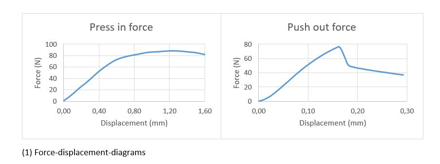 The metallographic inspection of the connections is guided by both supplier guidelines and IPC standards that define acceptable and unacceptable error patterns inside the PCBs. By measuring the remaining thickness of the via metallization (Figure 2) and the jet effect (Figure 3) pass or fail decisions can be made.
 Another risk is the formation of whiskers (Figure 4): long needle-like metallic structures that can reach millimeters in length and are thus able to short-circuit pins on PCBAs. Whenever tin-plated structures are exposed to mechanical forces, the growth of whiskers can start.Temperature cycling or humidity-temperature storage can accelerate the formation of whisker growth, which usually happens only in years. This enables us to perform an assessment after a few weeks. 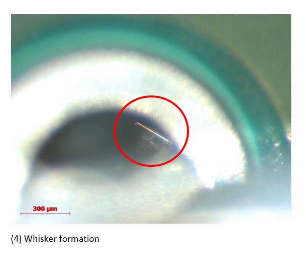 Our expertise and quality enjoy an excellent reputation, which is why we are one of only two approved laboratories of a major supplier. Contact us to find out more! |
||
RoodMicrotec GmbH | Oettinger Str. 6 | 86720 Nördlingen/ Germany Tel.: +49 (0) 9081 804-0 | [email protected] |
||
| If you no longer wish to receive our newsletter, please unsubscribe here | ||