News from RoodMicrotec
| This mail contains images. Alternatively you can watch the web version | ||
 |
||
| www.roodmicrotec.com | | ||
| Dear Reader, We are happy to present this year's first issue of RoodMicrotec's newsletter. In this edition, we will inform you about high voltage wafer & component testing and customized small batch packaging solutions.
Additionally, we want you to get to know us better. In every issue, there is going to be an insight interview with one of our experts. The first talk is done with Jessica Nogger of the Human Resources Department. It deals with the corona crisis and the challenges associated with it. Enjoy reading! We wish you all the best, your RoodMicrotec team! |
||
Packaging and Test of GaN power electronics Cost-effective power solutions for SMEs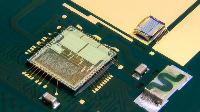 Figure 1: The power package for transistor and driver was produced by using generic chip-mold tools. (Source: RM) High-performance electronics is one of today's major emerging markets in the electronics industry. Electromobility, miniaturisation and increased efficiency are driving the development of new material systems such as gallium nitride (GaN) or silicon carbide (SiC). However, new materials with previously unattained properties are require new developments in the field of packaging and testing. As part of the BMBF-funded KMU-innovativ project GaNScan, RoodMicrotec has been working with its partners IMS Chips and AdMOS on various issues relating to GaN high-performance transistors over the past few years. In the project, the following tasks were included: IMS Chips developed a GaN-based high electron mobility transistor (HEMT) and designed a suitable driver ASIC. AdMOS developed a compact model from initial measurement data. RoodMicrotec has designed a package for transistor and driver and developed test methods for a high-voltage wafer test as well as a robust component test. The factors for a high-volume package and the realization of wafer and component tests that function up to 2000 V are described below. Low-Cost Custom Power Package for Intelligent GaN Transistors The functional and parametric qualification of a GaN transistor requires a suitable transistor package. For this purpose, the universal GaN driver chip was integrated together with the GaN transistor in a "System-in-Package" (SIP) package. This results in an exemplary intelligent and universal GaN transistor which in this form can perfectly be fitted into industrial applications. The GaNScan study successfully demonstrates that a suitable application-specific power package can be produced with low initial and development costs within the budget of a medium-sized company. Voltages of 650 V to 1000 V and pulsed currents of up to 100 A occur at the power transistor, depending on transistor type and size. With large-area GaN transistors, the package must have a low thermal resistance so that the power dissipation can be conducted away well at higher operating currents. 1000 V require a distance of at least 5 mm between the high-voltage connections. The versatile power package shown here is produced using generic chip-mold tooling, which completely eliminates tooling costs and limits setup costs. For this purpose, the dies are mounted on a PCB using "chip-on-board" (COB) technology together with passive components, where they are then bonded to gold-plated pads (see cover picture). With the available moulding tool, 33 chips can be moulded on a common substrate panel and separated (sawn out) after hardening. Before this, the panel is labeled with a laser. 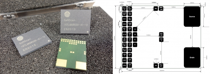 Figure 2: GaNScan prototype SiP LGA and pad drawing. (Source: RM) Additionally, an HV voltage divider and 2 decoupling capacitors for the 5 V operating voltage of the driver chip are integrated in the package. On the bottom side of the compact chip package (15x19x1.4 mm³), five HV connectors are arranged with 5 mm distance to each other and further 28 NV connectors for digital/analogue purposes. The large area source and drain solder pads transfer both a high current and the corresponding heat dissipation to the PCB thus, theoretically pulse currents up to 100 A are possible. With the current GaN SIP package design, switched-mode power supplies, intelligent high-voltage switches and motor controllers can be elegantly and economically built as a single chip solution. The package is soldered in normal surface mount soldering equipment and is absolutely suitable for mass production. Wafer Test Setup for GaN and SiC Power Semiconductors The challenges in wafer testing of power semiconductors lie in the naturally high voltages and currents. Needle boards are of particular importance as they are literally at the forefront of testing. With standard pin cards, for example, there is a risk of high-voltage flashovers and increased leakage currents. For on-wafer performance tests, we rely on a system consisting of a fully isolated HV motherboard and product-specific probe heads with advanced cantilever needles. The motherboard is specified for test voltages up to 3 kV and offers 14 HV channels as well as 30 low leakage channels (5 fA/V). The probe heads are based on ceramic cores and allow testing up to 200°C. To avoid high-voltage flashovers, the needles are equipped with a special coating. 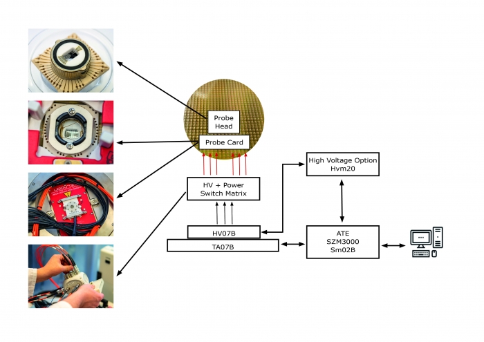 Figure 3: Structure and components of an HV wafer test. (Source: RM) High-voltage upgrade of a wafer prober The installed 8"/6" standard wafer probers are usually suitable for tests up to approx. 60 V. To ensure that the modification of a prober for up to 2000 V does not affect the prober's measuring equipment, controls or even the operating personnel, extensive measures are required. On one hand, it must be prevented that voltage flashovers occur on the control lines during operation, since even small induction voltages can have a negative influence on the sensitive positioning systems. On the other hand, the safety devices are of great importance when high voltages are involved. A hazard to the operating personnel must be excluded in accordance with accident prevention regulations. If a flap is opened during the test run, an immediate shutdown of the high voltage will take place. In addition, Normally-Closed relays discharge the cables from the tester to the probe card. As an additional benefit, the shielding and reinforced ground connections of the HV upgrade render the possibility of testing with high currents of up to 100 A in the forward range. With the upgrade, the prober meets the following specifications: - High Voltage: 0-3000VDC @ 3A or 10 k Watts, steady-state testing (100% duty cycle)
- High Voltage: 3000 V @ 10 A, 1-10 ms pulse (10% duty cycle)
- Low Voltage: 0-50 VDC @ 100 A, 10-20 ms pulse (10% duty cycle)
- CE certified and compliant
- SEMI-S2 compliant
Device test setup for packaged GaN and SiC power semiconductors
Test solutions for packaged power semiconductors require a robust setup. For contacting, the most important part besides the load board (as hardware interface to the tester) is the test socket. Since the device to be tested was a customised LGA package, also a customised socket had to be developed. The contacting was done via small spring pins. Due to the high currents, 4-wire or Kelvin contacting had to be used. In order to be able to transfer these currents safely during the test, several spring pins for Force and one each for Sense were placed on the large LGA pads (Drain + Source). For an extended temperature range, the test socket has an opening in the lid as well as small air flow channels. This optimises the temperature control by means of a thermostreamer and allows reproducible measurements in the range from -40°C to +150°C. As with the wafer test, high voltages of up to 2000 V are used to test the packaged components. For the safety of the operating personnel, several mechanisms are also implemented here that trigger immediate shutdowns in the event of incorrect operation. 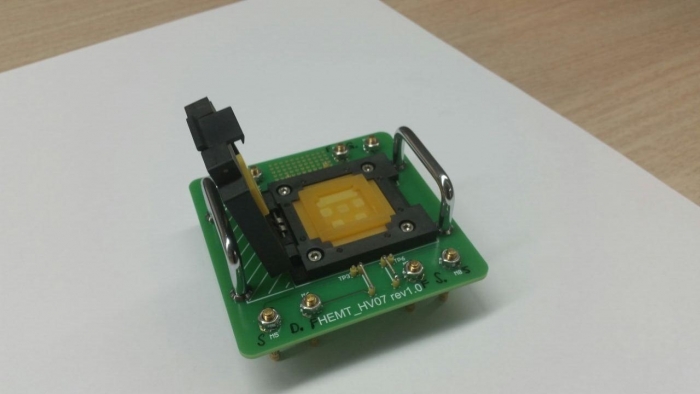 Figure 4: High-power test socket for GaN-HEMT in the package. (Source: RM) Test performance for GaN power semiconductors At the characterisation stage of GaN processes, parameters measured on the wafer such as contact and sheet resistance provide information about the quality. While a narrow distribution of the sheet resistance confirms the homogeneity of the 2DEG channel, ohmic contacts with an Rc < 1Ω∙mm indicate high-performance transistors. For production testing of GaN power semiconductors, the usual transistor parameters, such as drain-source leakage and RDS(ON), are used. What do you have to consider when testing GaN devices? A characteristic property of GaN is known as the "trapping effect" or "current collapse phenomenon". This behaviour degrades the achievable output power and linearity of the transistor. The undesired effect can be provoked by applying a high drain-source voltage in the off-state. A quality statement on this can be achieved during the test procedure by a voltage stress test via the detection of the RDS(on) change. For this purpose, the RDSon is determined first. Immediately afterwards, a drain-source stress voltage is applied for a few milliseconds in the off state directly followed by a second RDSon measurement. "Threshold shift" is another typical property of AlGaN/GaN high-electron-mobility transistors (HEMTs). This is caused by gate-source stress. To avoid measurement errors, it is therefore important not to apply high gate voltages during or before the threshold measurement. Conclusion: GaN power electronics require specialised packaging and test methods, both at wafer and component level. RoodMicrotec has developed the appropriate services for this. |
||
Interview with Jessica Nogger about the importance and challenges of Human Resources during the Corona pandemic Jessica Nogger is responsible for all topics concerning Human Resources. She started her career at RoodMicrotec in 2011. This year she celebrates her 10th anniversary. What concerns do you have at the moment? What challenges does HR face in times of corona? Currently, I am concerned about the vaccination delay or rather how slowly vaccinations are administered. The easing of restrictions and openings solely depends on the vaccinations and the longer it takes the more likely a third wave could indeed still be "rolling towards us". What worries me the most is an infection of a staff member, especially what this would mean for internal contacts, quarantine, etc. I am glad that I am able to continue to be on site in the office to be there for the staff. In the future, the main challenge for recruitment will be to come into contact with the candidate, or rather to use appropriate tools such as Zoom/Teams/Skype to get closest to a face-to-face meeting in the first interview. Why has HR become even more relevant in times of Corona? We are and will remain the contact persons for our employees, no matter what issues or concerns they have, our door is open for everyone and we also are available for everyone by phone/ Skype/ Zoom/ Teams. It is a strange time for everyone and there are various uncertainties we would like to clarify in order to continuously motivate our employees. Of course, the topic of short-time work also is a problem for our employees. Concerning this matter, we try to clarify all open questions and always thank them for their support! How have the tasks of the HR department changed since the start of the pandemic? HR has become even more a point of contact for questions and "concerns" since the outbreak of Corona. Not only because of the constantly changing Corona directives or short-time work. But by being present in the office, we can also provide a little bit of tranquility and "structure". To what extent does Corona promote or inhibit ‘New Work’ efforts at RoodMicrotec? Corona has increasingly enabled us to work from home or on the move. This was/is not only a big challenge for IT, but also for the supervisors, as they now have to manage their teams differently. However, the way is now paved for further support this, to move away from mere conference calls to more zoom / team meetings, as especially video conferences give the feeling of being in the same room. While I still think on-site collaboration is most important, I hope we can use video conferences to improve collaboration between sites. What do you like about your job? / What is annoying? I'm excited about working with colleagues and managers, providing advice and support to everyone, and to be able to contribute a little bit to the good atmosphere in the company. My work in HR is very diverse, there are no two days alike and there are always new issues and challenges that I enjoy tackling. I would be annoyed if I had to do the same thing every day and if work got boring, but fortunately, this doesn’t happen ? 6. What do you do when you’re not working? Then, I’m mainly fetching coffee and seek contact with colleagues, always observing the AHA rules, of course. 7. What do you wish for the future? A cautious path back to normality, even if things will never be the same as they were before Corona. |
||
RoodMicrotec GmbH | Oettinger Str. 6 | 86720 Nördlingen/ Germany Tel.: +49 (0) 9081 804-0 | [email protected] |
||
| If you no longer wish to receive our newsletter, please unsubscribe here | ||